Korea Institute of Energy Research
Korea Institute of Energy Research (KIER)
Thin-Film Silicon Integrated Back-Contact Electrode Technology for Perovskite Solar Cells
Integrated Back-Contact Electrode Technology That Simultaneously Extends the Lifespan and Increases the Power-Generating Area of Perovskite Solar Cells by Consolidating All Electrodes on the Back Side
Technology Overview
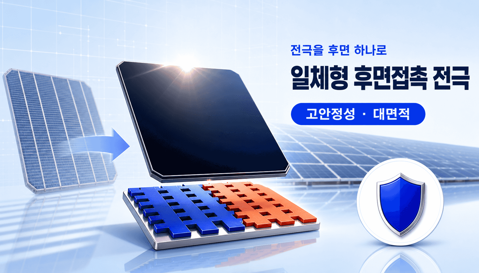
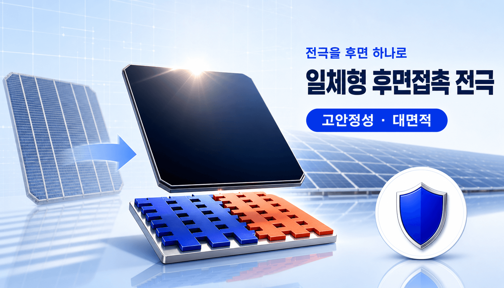
Monolithic Back Contact (MBC) electrode technology that integrates the hole transport layer (HTL), electron transport layer (ETL), anode, and cathode functions of perovskite solar cells onto a single back substrate
Replaces the organic charge transport layers—which have long been the primary cause of long-term stability degradation, the biggest obstacle to commercialization—with thin-film silicon, a material already proven in the semiconductor and display industries
Maximizes the light-receiving area by eliminating the front electrodes and dead area
Technology Configuration
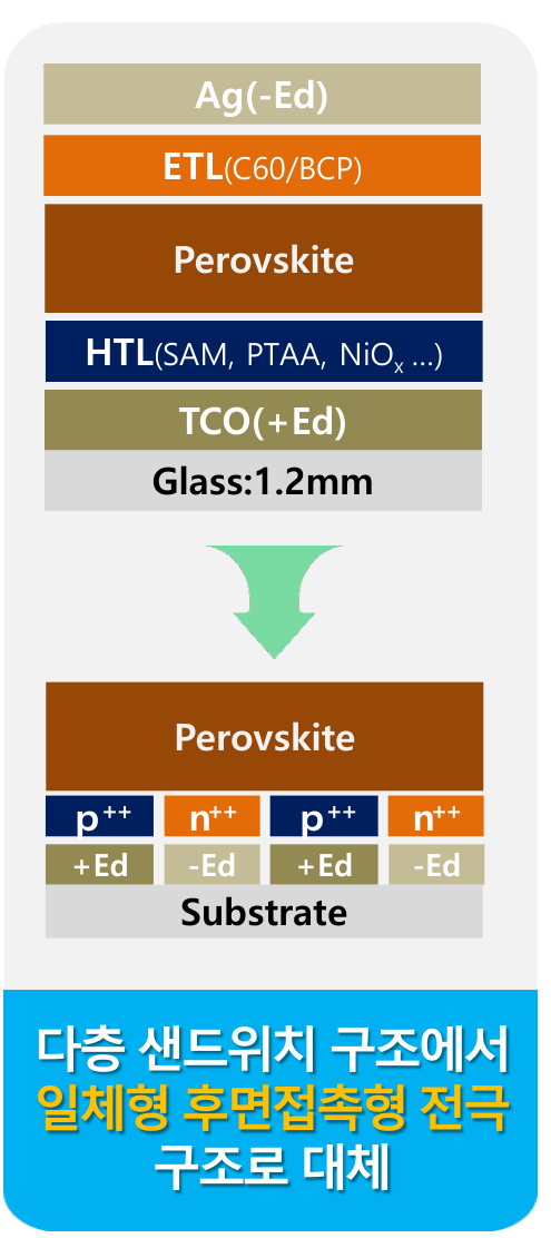
Instead of the conventional sandwich-type multilayer thin-film structure, the hole collection region (p⁺⁺) and electron collection region (n⁺⁺) are patterned side-by-side on the back substrate with line widths of several µm, integrated into a single electrode, and a perovskite light-absorbing layer is formed on top
Key Technology Features
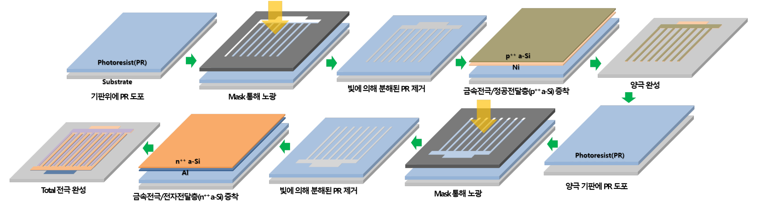
Process technology for depositing a thin-film silicon charge-transport layer under low-temperature, low-power plasma conditions that do not damage the perovskite light-absorbing layer (substrate temperature below 150 °C; suppression of damage to the underlying film caused by hydrogen radicals through adjustment of gas composition ratios)
High-precision electrode patterning technology in the range of several µm that electrically insulates the hole collection and electron collection sections while arranging them side-by-side on the rear surface (using lift-off, photolithography, and etching)
Design technology that optimizes charge collection efficiency by deriving electrode line widths and spacings via simulation, taking into account the grain size of the light-absorbing layer
Technology for achieving large-area devices of 200 cm² or more using semiconductor foundry processes
Comparative Advantages of the Technology
Existing Technology | This Technology |
The use of organo-inorganic materials with low stability in the charge transfer layer leads to degradation caused by thermal decomposition, UV exposure, interfacial instability, and ion migration | Thin-film silicon, proven to be stable in semiconductors and displays, is used as the charge transport layer, and the dense thin-film structure blocks moisture penetration and elemental diffusion |
Since the front and back electrodes are arranged separately, light loss occurs due to front grid shading and dead areas; furthermore, TCO accounts for 30–40% of the device cost | By integrating both electrodes onto the back substrate, front-side shading is eliminated to maximize the light-receiving area, and low-cost metals such as Al and Cu can be used as alternatives to TCO |
Since multi-layer thin films—which are sensitive to process conditions—must be deposited in a continuous process, interfacial damage and yield degradation occur, and quality variations increase as the area is scaled up | Separating the electrode formation process from the light-absorbing layer formation process ensures process flexibility, while semiconductor patterning ensures uniformity across large areas. |
Applications
| Application Fields | Applicable Products |
|---|---|
|
|
TRL Stage
- 1
- 2
- 3
- 4
- 5
- 6
- 7
- 8
- 9
TRL 2–3
The feasibility of using thin-film silicon as a perovskite charge-transport layer has been demonstrated in previous studies.